Anyone involved within the printed circuit board (PCB) industry understand that PCBs have copper finishes on their surface. If they are left unprotected then the copper will oxidize and deteriorate, making the circuit board unusable. The surface finish forms a critical interface between the component and the PCB. The finish has two essential functions, to protect the exposed copper circuitry and to provide a solderable surface when assembling (soldering) the components to the printed circuit board.
HASL / Lead Free HASL
HASL is the predominant surface finish used in the industry. The process consists of immersing circuit boards in a molten pot of a tin/lead alloy and then removing the excess solder by using 'air knives', which blow hot air across the surface of the board.
One of the unintended benefits of the HASL process is that it will expose the PCB to temperatures up to 265°C which will identify any potential delamination issues well before any expensive components are attached to the board.

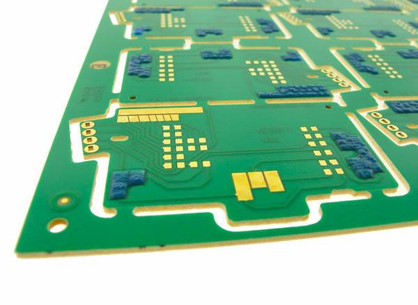
HASL Finished Double Sided Printed Circuit Board
Advantages:
-
Low Cost
-
Widely Available
-
Re-workable
-
Excellent Shelf Life
Disadvantages:
-
Uneven Surfaces
-
Not Good for Fine Pitch
-
Contains Lead (HASL)
-
Thermal Shock
-
Solder Bridging
-
Plugged or Reduced PTH's (Plated Through Holes)
Immersion Tin
According to IPC, the Association Connecting Electronics Industry, Immersion Tin (ISn) is a metallic finish deposited by a chemical displacement reaction that is applied directly over the basis metal of the circuit board, that is, copper. The ISn protects the underlying copper from oxidation over its intended shelf life.
Copper and tin however have a strong affinity for one another. The diffusion of one metal into the other will occur inevitably, directly impacting the shelf life of the deposit and the performance of the finish. The negative effects of tin whiskers growth are well described in industry related literature and topics of several published papers.
Advantages:
-
Flat Surface
-
No Pb
-
Re-workable
-
Top Choice for Press Fit Pin Insertion
Disadvantages:
-
Easy to Cause Handling Damage
-
Process Uses a Carcinogen (Thiourea)
-
Exposed Tin on Final Assembly can Corrode
-
Tin Whiskers
-
Not Good for Multiple Reflow/Assembly Processes
-
Difficult to Measure Thickness
Immersion Silver
Immersion silver is a non-electrolytic chemical finish applied by immersing the copper PCB into a tank of silver ions. It is a good choice finish for circuit boards with EMI shieldingand is also used for dome contacts and wire bonding. The average surface thickness of the silver is 5-18 microinches.
With modern environmental concerns such as RoHS and WEE, immersion silver is environmentally better than both HASL and ENIG. It is popular also due to its lesser cost than ENIG.

Advantages:
-
Applies more evenly than HASL
-
Environmentally better than ENIG and HASL
-
Shelf life equal to HASL
-
More cost-effective than ENIG
Disadvantages:
-
Must be soldered within the day the PCB is removed from storage
-
Can be tarnished easily with improper handling
-
Less durable than ENIGdue to no layer of nickel underneath
OSP / Entek
OSP (Organic Solderability Preservative) or anti-tarnish preserves the copper surface from oxidation by applying a very thin protective layer of material over the exposed copper usually using a conveyorized process.
It uses a water-based organic compound that selectively bonds to copper and provides an organometallic layer that protects the copper prior to soldering. It's also extremely green environmentally in comparison with the other common lead-free finishes, which suffer from either being more toxic or substantially higher energy consumption.
Advantages:
-
Flat Surface
-
No Pb
-
Simple Process
-
Re-workable
-
Cost Effective
Disadvantages:
-
No Way to Measure Thickness
-
Not Good for PTH (Plated Through Holes)
-
Short Shelf Life
-
Can Cause ICT Issues
-
Exposed Cu on Final Assembly
-
Handling Sensitive
Electroless Nickel Immersion Gold (ENIG)
ENIG is a two layer metallic coating of 2-8 μin Au over 120-240 μin Ni. The Nickel is the barrier to the copper and is the surface to which the components are actually soldered to. The gold protects the nickel during storage and also provides the low contact resistance required for the thin gold deposits. ENIG is now arguably the most used finish in the PCB industry due the growth and implementation of the RoHs regulation.

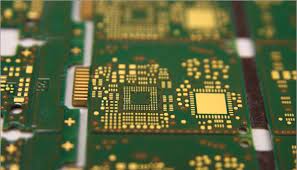
Printed Circuit Board with Chem Gold Surface Finish
Advantages:
-
Flat Surface
-
No Pb
-
Good for PTH (Plated Through Holes)
-
Long Shelf Life
Disadvantages:
-
Expensive
-
Not Re-workable
-
Black Pad / Black Nickel
-
Damage from ET
-
Signal Loss (RF)
-
Complicated Process
Electroless Nickel Electroless Palladium Immersion Gold (ENEPIG)
ENEPIG, a relative newcomer to the circuit board world of finishes, first came on the market in the late 90s. This three-layer metallic coating of nickel, palladium, and gold provides an option like no others: it is bondable. ENEPIG’s first crack at a printed circuit board surface treatment fizzled with manufacturing due to its extreme high cost layer of palladium and low demand of use.
The need for a separate manufacturing line was not receptive for these same reasons. Recently, ENEPIG has made a comeback as the potential to meet reliability, packaging needs, and RoHS standards are a plus with this finish. It is perfect for high frequency applications where spacing is limited.
When compared to the other top four finishes, ENIG, Lead Free-HASL, immersion silver and OSP, ENEPIG outperforms all on the after-assembly corrosion level.
Advantages:
-
Extremely Flat Surface
-
No Lead Content
-
Multi-Cycle Assembly
-
Excellent Solder Joints
-
Wire Bondable
-
No Corrosion Risks
-
12 Month or Greater Shelf Life
-
No Black Pad Risk
Disadvantages:
-
Still Somewhat More Expensive
-
Is Re-Workable with Some Limitations
-
Processing Limits
Gold – Hard Gold
Hard Electrolytic Gold consists of a layer of gold plated over a barrier coat of nickel. Hard gold is extremely durable, and is most commonly applied to high-wear areas such as edge connector fingers and keypads.
Unlike ENIG, its thickness can vary by controlling the duration of the plating cycle, although the typical minimum values for fingers are 30 μin gold over 100 μin nickel for Class 1 and Class 2, 50 μin gold over 100 μin nickel for Class 3.
Hard gold is not generally applied to solderable areas, because of its high cost and its relatively poor solderability. The maximum thickness that IPC considers to be solderable is 17.8 μin, so if this type of gold must be used on surfaces to be soldered, the recommended nominal thickness should be about 5-10 μin.
Advantages:
-
Hard, Durable Surface
-
No Pb
-
Long Shelf Life
Disadvantages:
-
Very Expensive
-
Extra Processing / Labor Intensive
-
Use of Resist / Tape
-
Plating / Bus Bars required
-
Demarcation
-
Difficulty with Other Surface Finishes
-
Etching Undercut can Lead to Slivering / Flaking
-
Not Solderable Above 17 μin
-
Finish Does Not Fully Encapsulate Trace Sidewalls, Except in Finger Areas
Looking for a Special Surface Finish for Your Circuit Board?


 Englishen


