PCB Manufacturing Process: From Concept to Assembly
Printed Circuit Boards (PCBs)are the foundation of electronic devices, facilitating the connection between various components. The journey from conceptualizing a design to assembling a functional PCB involves a series of intricate steps. In this blog post, we'll take a comprehensive look at the PCB manufacturing process, highlighting the key stages that transform a design on paper into a fully functional circuit board.
1.Design and Layout
The process begins with the conceptualization of the electronic device and the creation of a schematic diagram. Engineers use specialized software to design the circuit, considering factors such as component placement, signal paths, and power distribution.
Once the schematic is finalized, the PCB layout is designed. This involves placing components on the board, routing traces, and defining the layer stackup. The layout must adhere to principles that ensure optimal signal integrity, thermal management, and manufacturability.
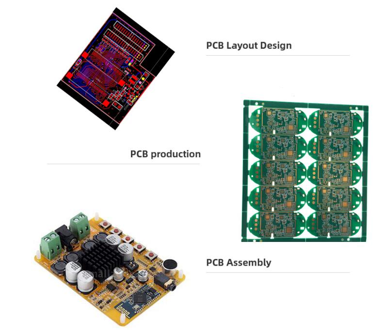
2.Gerber Files and Manufacturing Preparation
The PCB layout is then converted into Gerber files, which contain the necessary information for manufacturing. These files specify the layers, traces, and other critical details required for the fabrication process.
-
Design for Manufacturing (DFM) Check:
Before moving forward, a Design for Manufacturing (DFM) check is performed to identify and address any potential issues that may arise during fabrication. This step ensures that the design is manufacturable and minimizes the risk of errors in the final product.

3.PCB Fabrication
The chosen substrate material, often fiberglass-reinforced epoxy known as FR-4, is prepared for the manufacturing process. Copper layers are laminated onto the substrate, forming the basis of the conductive pathways.
-
Photoresist Application and Imaging:
A layer of photoresist is applied to the copper surface. The Gerber files are then used to create a photomask, which is used to expose the areas where copper should be etched away. This step defines the copper traces and pads on the board.
The exposed PCB is submerged in an etchant, which removes the unwanted copper, leaving behind the desired circuit pattern. This process is crucial for shaping the conductive paths on the board.
After etching, holes are drilled to accommodate through-hole components and vias. These holes are then plated with a conductive material to establish electrical connections between different layers of the PCB.


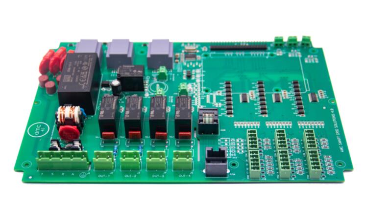
4.PCB Assembly (PCBA)
The fabricated PCB is now ready for assembly. Components, such as resistors, capacitors, and integrated circuits, are placed on the board according to the assembly plan.
The components are soldered onto the PCB using surface mount technology (SMT) or through-hole technology (THT). Soldering creates electrical connections and ensures the components are securely attached to the board.
Once assembled, the PCB undergoes rigorous inspection and testing processes. Automated optical inspection (AOI) and functional testing verify the integrity of the connections and the functionality of the electronic device.
Conclusion
The journey from a conceptualized circuit to a fully functional PCB involves a meticulous and multi-step process. Each stage, from design and layout to fabrication and assembly, requires precision and attention to detail. By understanding these key stages, engineers can ensure the successful manufacture of high-quality PCBs that power a diverse range of electronic devices. The collaboration between design expertise and advanced manufacturing technologies continues to drive innovation in the realm of PCBs, shaping the future of electronic devices.


 Englishen


