How is the circuit board of the PCB factory made? The small circuit material that can be seen on the surface is copper foil. Originally, the copper foil was covered on the entire PCB, but part of it was etched away during the manufacturing process, and the remaining part became a mesh-like small circuit. .
These lines are called wires or traces and are used to provide electrical connections to components on the PCB. Usually the color of the
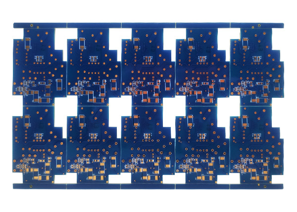
PCB board is green or brown, which is the color of the solder mask. It is an insulating protective layer that protects the copper wire and also prevents parts from being soldered to incorrect places.
Multilayer Circuit boards are now used on motherboards and graphics cards, which greatly increases the area that can be wired. Multilayer boards use more
single or double-sided wiring boards, and put an insulating layer between each board and press them together. The number of layers of the PCB board means that there are several independent wiring layers, usually the number of layers is even, and includes the outermost two layers. Common PCB boards are generally 4 to 8 layers of structure. The number of layers of many PCB boards can be seen by viewing the section of the PCB board. But in reality, no one has such a good eye. So, here's another way to teach you.
The circuit connection of multi-layer boards is through buried via and blind via technology. Most motherboards and display cards use 4-layer PCB boards, and some use 6-, 8-layer, or even 10-layer PCB boards. If you want to see how many layers there are in the PCB, you can identify it by observing the guide holes, because the 4-layer boards used on the main board and the display card are the first and fourth layers of wiring, and the other layers are used for other purposes (ground wire). and power).
Therefore, like the double-layer board, the guide hole will penetrate the PCB board. If some vias appear on the front side of the PCB but cannot be found on the reverse side, then it must be a 6/8-layer board. If the same guide holes can be found on both sides of the PCB board, it is naturally a 4-layer board.
The PCB manufacturing process begins with a PCB "substrate" made of Glass Epoxy or similar. The first step of production is to draw the wiring between the parts. The method is to "print" the circuit negative of the designed PCB circuit board on the metal conductor by means of Subtractive transfer.
The trick is to spread a thin layer of copper foil over the entire surface and remove the excess. If the production is double-sided, then both sides of the PCB substrate will be covered with copper foil. To make a multi-layer board, the two double-sided boards can be "pressed" together with a special adhesive.
Next, the drilling and electroplating required to connect components can be performed on the PCB board. After drilling by machine equipment according to drilling requirements, the inside of the hole wall must be plated (Plated-Through-Hole technology, PTH). After the metal treatment is performed inside the hole wall, the internal layers of circuits can be connected to each other.
Before starting electroplating, the debris in the hole must be cleaned. This is because the resin epoxy will undergo some chemical changes when heated, and it will cover the inner PCB layers, so it needs to be removed first. Both the cleaning and plating actions are done in the chemical process. Next, it is necessary to coat the solder resist paint (solder resist ink) on the outermost wiring so that the wiring does not touch the plated part.
Then, various components are screen-printed on the circuit board to indicate the position of each part. It cannot cover any wiring or gold fingers, otherwise it may reduce the solderability or the stability of the current connection. In addition, if there are metal connections, the "gold fingers" are usually plated with gold at this time to ensure a high-quality electrical connection when inserted into the expansion slot.

Finally, there is the test. Test the PCB for shorts or open circuits, either optically or electronically. Optical methods use scanning to find defects in each layer, and electronic testing usually uses a Flying-Probe to check all connections. Electronic testing is more accurate at finding shorts or opens, but optical testing can more easily detect problems with incorrect gaps between conductors.
After the circuit board substrate is completed, a finished motherboard is equipped with various components of various sizes on the PCB substrate according to the needs - first use the SMT automatic placement machine to "solder the IC chip and the patch components", and then manually connect. Plug in some work that cannot be done by the machine, and firmly fix these plug-in components on the PCB through the wave/reflow soldering process, so a motherboard is produced.


 Englishen


