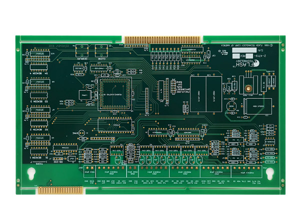
The output value of the global electroplating PCB industry has grown rapidly in the total output value of the electronic component industry. It is the industry with the largest proportion in the electronic component subdivision industry and occupies a unique position. The annual output value of electroplating PCB is 60 billion US dollars. The volume of electronic products is becoming more and more thin and short, and the direct stacking of vias on through-blind vias is a design method to obtain high-density interconnection. To do a good stacking hole, first of all, the flatness of the hole bottom should be done well. There are several ways to make a typical flat hole surface, and the electroplating hole filling process is a representative one.
In addition to reducing the need for additional process development, the electroplating and hole filling process is also compatible with current process equipment, which is conducive to obtaining good reliability.
Electroplating hole filling has the following advantages:
(1) It is beneficial to design Stacked and Via.on.Pad (HDI Circuit Board);
(2) Improve electrical performance and help high-frequency design;
(3) Helps to dissipate heat;
(4) The plug hole and electrical interconnection are completed in one step;
(5) The blind holes are filled with electroplated copper, which has higher reliability and better conductivity than conductive glue.

Physical Influence Parameters
The physical parameters to be studied are: anode type, cathode-anode spacing, current density, agitation, temperature, rectifier and waveform, etc.
(1) Anode type. When it comes to anode types, it is nothing more than soluble anodes and insoluble anodes. Soluble anodes are usually phosphorus-containing copper balls, which are easy to produce anode slime, pollute the plating solution, and affect the performance of the plating solution. Insoluble anodes, also known as inert anodes, generally consist of a titanium mesh coated with mixed oxides of tantalum and zirconium. Insoluble anode, good stability, no anode maintenance, no anode sludge, suitable for pulse or DC electroplating; however, the consumption of additives is large.
(2) The distance between cathode and anode. The spacing design between the cathode and the anode in the electroplating via filling process is very important, and the design of different types of equipment is also different. However, it should be pointed out that no matter how it is designed, it should not violate Fara's first law.
(3) Stirring. There are many types of stirring, such as mechanical shaking, electric vibration, gas vibration, air stirring, Eductor and so on.
For electroplating and filling, it is generally preferred to increase the jet design based on the configuration of the traditional copper cylinder. However, whether it is the bottom jet or the side jet, how to arrange the jet tube and the air stirring tube in the cylinder; what is the jet flow per hour; what is the distance between the jet tube and the cathode; if the side jet is used, the jet is at the anode Front or back; if the bottom jet is used, will it cause uneven stirring, and the plating solution will be weakly stirred up and down; To do a lot of testing.
In addition, the most ideal way is to connect each jet tube to the flow meter, so as to achieve the purpose of monitoring the flow. Due to the large jet flow, the solution is prone to heat, so temperature control is also important.
(4) Current density and temperature. Low current density and low temperature can reduce the deposition rate of surface copper, while providing sufficient Cu2 and brightener into the hole. Under these conditions, the hole filling capability is enhanced, but the plating efficiency is also reduced.
(5) Rectifier. The rectifier is an important link in the electroplating process. At present, the research on electroplating and filling is mostly limited to full-board electroplating. If the pattern electroplating and filling are considered, the cathode area will become very small. At this time, high requirements are put forward for the output precision of the rectifier.
The selection of the output precision of the rectifier should be determined according to the line of the product and the size of the via hole. The thinner the lines and the smaller the holes, the higher the accuracy requirements of the rectifier should be. Usually, it is advisable to choose a rectifier with an output accuracy within 5%. Selecting a rectifier that is too precise will increase the investment in the equipment. When wiring the output cable of the rectifier, first place the rectifier on the edge of the plating tank as much as possible, which can reduce the length of the output cable and reduce the rise time of the pulse current. The selection of the rectifier output cable specification should meet the line voltage drop of the output cable within 0.6V at 80% of the maximum output current. Usually, the required cable cross-sectional area is calculated according to the current carrying capacity of 2.5A/mm:. If the cross-sectional area of the cable is too small, the cable length is too long, or the line voltage drop is too large, the transmission current will not reach the current value required for production.
For the plating tank with a tank width greater than 1.6m, the method of bilateral power feeding should be considered, and the length of the bilateral cables should be equal. In this way, the bilateral current error can be guaranteed to be controlled within a certain range. A rectifier should be connected to both sides of each flybar of the plating tank, so that the current on the two sides of the piece can be adjusted separately.
(6) Waveform. At present, from the waveform point of view, there are two types of electroplating and filling: pulse electroplating and DC electroplating. These two methods of electroplating and hole filling have been studied. The traditional rectifier is used for DC electroplating and hole filling, which is easy to operate, but if the plate is thicker, there is nothing that can be done. PPR rectifier is used for pulse electroplating and hole filling, which has many operation steps, but has strong processing ability for thicker in-process boards.
The influence of the substrate
The influence of the substrate on electroplating and hole filling cannot be ignored. Generally, there are factors such as dielectric layer material, hole shape, aspect ratio, and chemical copper plating.
(1) Dielectric layer material. The material of the dielectric layer has an effect on hole filling. Non-glass reinforcements are easier to fill holes than glass fiber reinforcements. It is worth noting that the glass fiber protrusions in the hole have a detrimental effect on chemical copper. In this case, the difficulty of electroplating hole filling is to improve the adhesion of the electroless plating seed layer, rather than the hole filling process itself.
In fact, electroplating and filling holes on glass fiber reinforced substrates have been applied in actual production.
(2) Aspect ratio. At present, the hole filling technology for holes of different shapes and sizes is highly valued by both manufacturers and developers. The hole filling ability is greatly affected by the hole thickness to diameter ratio. Relatively speaking, DC systems are used more commercially. In production, the size range of the hole will be narrower, generally the diameter is 80pm~120Bm, the hole depth is 40Bm~8OBm, and the thickness-diameter ratio does not exceed 1:1.
(3) Electroless copper plating layer. The thickness and uniformity of the electroless copper plating layer and the standing time after electroless copper plating all affect the hole filling performance. Electroless copper is too thin or has uneven thickness, and its hole filling effect is poor. Generally, it is recommended to fill holes when the thickness of chemical copper is > 0.3pm. In addition, the oxidation of chemical copper also has a negative impact on the hole filling effect.


 Englishen


