What Is Silkscreen On a PCB?
When you design or order your printed circuit boards, do you need to pay extra for silkscreen? There are some questions you need to know what’s silkscreen? And how important silkscreen is in your PCB Board fabrication or Printed Circuit Board Assembly? Now ABIS will explain for you.
What is silkscreen?
Silkscreen is a layer of ink traces used to identify components, test points, parts of the PCB, warning symbols, logos and marks etc. This silkscreen is usually applied on the component side; however using silkscreen on the solder side is also not uncommon. But this may increase the cost. Essentially a detailed PCB silkscreen can help both the manufacturer and the engineer to locate and identify all the components.
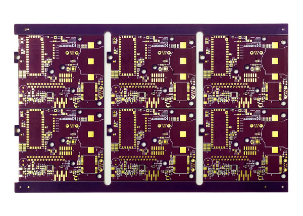
The ink is a non-conductive epoxy ink. The ink used for these markings is highly formulated. The standard colors we normally see are black, white and yellow. PCB software also uses standard fonts in silkscreen layers but you can choose other fonts from the system too. For traditional silk-screening you require a polyester screen stretched on aluminum frames, a laser photo plotter, spray developer and curing ovens.
What will affect silkscreen?
Viscosity: Viscosity refers to the relative movement between adjacent fluid layers when the fluid is flowing, then frictional resistance will be generated between the two fluid layers; unit: Pascal seconds (pa.s).
Hardness: The hardness of the ink after the pre-baking is 2B, the hardness of the ink after the exposure is 2H, and the hardness of the ink after the post-baking is 6H. Pencil hardness.
Thixotropic: the ink is gelatinous when standing, but the viscosity changes when touched, also known as thixotropic, anti-sagging; it is a physical property of the liquid, that is, in the state of stirring Its viscosity drops, and it quickly recovers its original viscosity characteristics after being allowed to stand. Through stirring, the effect of thixotropy lasts for a long time, enough to rebuild its internal structure. To achieve high-quality screen printing results, the thixotropy of the ink is very important. Especially in the process of squeegee, the ink is agitated to make it liquefied. This effect accelerates the speed of ink passing through the mesh, and promotes the uniform connection of the ink separated by the mesh. Once the squeegee stops moving, the ink returns to a static state, and its viscosity quickly returns to the original required data.
Dry film:
Dry film structure:
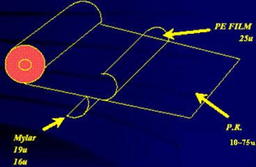
Dry film consists of three parts and ingredients:
Support film (polyester film, Polyester)
Photo-resist Dry Film
Cover film (polyethylene film, Polyethylene)
Main ingredients
①Binder binder (film-forming resin),
②Photo-polymerization monomer Monomer,
③Photo-initiator,
④Plasticiser,
⑤Adhesion Promoter,
⑥Thermal polymerization inhibitor,
⑦Pigment Dye,
⑧ solvent
The dry film types are divided into three categories according to the dry film development and removal methods: solvent-based dry film, water-soluble dry film and peel-off dry film; according to the purpose of the dry film, it is divided into: resist dry film, masked dry film and Solder mask dry film.
Sensitivity speed: refers to the amount of light energy required for the photoresist to polymerize the photoresist to form a polymer with a certain resistance to resist under the irradiation of ultraviolet light, under the condition of fixed light source intensity and lamp distance , Sensitivity speed is expressed as the length of exposure time, short exposure time means fast sensitization speed.
Resolution: refers to the number of lines (or spacing) that can be formed by the dry film resist within a distance of 1mm. The resolution can also be expressed by the absolute size of the lines (or spacing).
Net yarn:
Net density:
T number: refers to the number of meshes within 1 cm length.


 Englishen


