The base material of the circuit board of the electro-acoustic PCB factory only has copper foil on both sides, and the middle is the insulating layer, so they do not need to be conductive between the Double sides or multi-layer circuits of the circuit board? How can the lines on both sides be connected together so that the current flows smoothly?
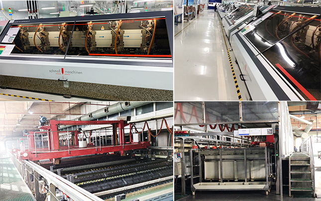
Below, please see the electroacoustic PCB manufacturer to analyze this magical process for you - copper sinking (PTH).
Immersion copper is the abbreviation of Eletcroless Plating Copper, also known as Plated Through Hole, abbreviated as PTH, which is an autocatalytic redox reaction. After the two-layer or multi-layer board is drilled, the PTH process is carried out.
The role of PTH: On the non-conductive hole wall substrate that has been drilled, a thin layer of chemical copper is chemically deposited to serve as the substrate for subsequent copper electroplating.
PTH process decomposition: alkaline degreasing → secondary or tertiary countercurrent rinsing → coarsening (micro-etching) → secondary countercurrent rinsing → presoak → activation → secondary countercurrent rinsing → degumming → secondary countercurrent rinsing → copper sinking → secondary stage countercurrent rinsing → pickling
PTH detailed process explanation:
1. Alkaline degreasing: remove oil stains, fingerprints, oxides, and dust in the pores; adjust the pore wall from negative charge to positive charge, which is convenient for the adsorption of colloidal palladium in the subsequent process; cleaning after degreasing must strictly follow the guidelines Carry out the test with the immersion copper backlight test.
2. Micro-etching: remove the oxides on the board surface, roughen the board surface, and ensure good bonding force between the subsequent copper immersion layer and the bottom copper of the substrate; the new copper surface has strong activity and can well adsorb colloids palladium;
3. Pre-dip: It is mainly to protect the palladium tank from the pollution of the pretreatment tank liquid and prolong the service life of the palladium tank. The main components are the same as those of the palladium tank except for palladium chloride, which can effectively wet the hole wall and facilitate the subsequent activation of the liquid. Enter the hole in time for sufficient and effective activation;
4. Activation: After the polarity adjustment of alkaline degreasing pretreatment, the positively charged pore walls can effectively absorb enough negatively charged colloidal palladium particles to ensure the uniformity, continuity and compactness of subsequent copper precipitation; Therefore, degreasing and activation are very important to the quality of subsequent copper deposition. Control points: specified time; standard stannous ion and chloride ion concentration; specific gravity, acidity and temperature are also very important, and they must be strictly controlled according to the operation instructions.
5. Degumming: remove the stannous ions coated on the outside of the colloidal palladium particles to expose the palladium core in the colloidal particles to directly and effectively catalyze the chemical copper precipitation reaction. Experience shows that it is better to use fluoroboric acid as the degumming agent. s Choice.
6. Copper precipitation: The electroless copper precipitation autocatalytic reaction is induced by the activation of the palladium nucleus. The newly formed chemical copper and the reaction by-product hydrogen can be used as reaction catalysts to catalyze the reaction, so that the copper precipitation reaction continues continuously. After processing through this step, a layer of chemical copper can be deposited on the board surface or the hole wall. During the process, the bath liquid should be kept under normal air agitation to convert more soluble bivalent copper.
The quality of the copper immersion process is directly related to the quality of the production circuit board. It is the main source process of poor vias, open and short circuits, and it is not convenient for visual inspection. The subsequent process can only be screened by destructive experiments. Effective analysis and monitoring of a single PCB board, so once a problem occurs, it must be a batch problem, even if the test cannot be completed, the final product will cause great hidden dangers to quality, and can only be scrapped in batches, so it must be strictly operated according to the parameters of the operation instructions.


 Englishen


