The key to PCB EMC design is to minimize the reflow area and let the reflow path flow in the direction of the design. The most common return current problems come from cracks in the reference plane, changing the reference plane layer, and the signal flowing through the connector.
Jumper capacitors or decoupling capacitors may solve some problems, but the overall impedance of capacitors, vias, pads, and wiring must be considered.
This article will introduce EMC's PCB design technology from three aspects: PCB layering strategy, layout skills and wiring rules.
PCB layering strategy
The thickness, via process and the number of layers in the circuit board design are not the key to solving the problem. Good layered stacking is to ensure the bypass and decoupling of the power bus and minimize the transient voltage on the power layer or ground layer. The key to shielding the electromagnetic field of the signal and power supply.
From the perspective of signal traces, a good layering strategy should be to put all signal traces on one or several layers, and these layers are next to the power layer or ground layer. For the power supply, a good layering strategy should be that the power layer is adjacent to the ground layer, and the distance between the power layer and the ground layer is as small as possible. This is what we are talking about "layering" strategy. Below we will specifically talk about a good PCB layering strategy.
1. The projection plane of the wiring layer should be in the area of the reflow plane layer. If the wiring layer is not in the projection area of the reflow plane layer, there will be signal lines outside the projection area during wiring, which will cause "edge radiation" problems, and will also increase the area of the signal loop, resulting in increased differential mode radiation .
2. Try to avoid setting up adjacent wiring layers. Because parallel signal traces on adjacent wiring layers can cause signal crosstalk, if adjacent wiring layers cannot be avoided, the layer spacing between the two wiring layers should be appropriately increased, and the layer spacing between the wiring layer and its signal circuit should be reduced.
3. Adjacent plane layers should avoid overlapping of their projection planes. Because when the projections overlap, the coupling capacitance between the layers will cause the noise between the layers to couple with each other.
Multilayer board design
When the clock frequency exceeds 5MHz, or the signal rise time is less than 5ns, in order to control the signal loop area well, a multi-layer board design is generally required. The following principles should be paid attention to when designing multilayer boards:
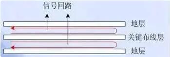
1. The key wiring layer (the layer where the clock line, bus, interface signal line, radio frequency line, reset signal line, chip select signal line and various control signal lines are located) should be adjacent to the complete ground plane, preferably between the two ground planes ,As shown in Figure 1.
Key signal lines are generally strong radiation or extremely sensitive signal lines. Wiring close to the ground plane can reduce the signal loop area, reduce its radiation intensity or improve anti-interference ability.
2. The power plane should be retracted relative to its adjacent ground plane (recommended value 5H~20H). The retraction of the power plane relative to its return ground plane can effectively suppress the "edge radiation" problem, as shown in Figure 2.
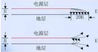
In addition, the main working power plane of the board (the most widely used power plane) should be close to its ground plane to effectively reduce the loop area of the power current, as shown in Figure 3.
3. Whether there is no signal line ≥50MHz on the TOP and BOTTOM layer of the board. If so, it is best to walk the high-frequency signal between the two plane layers to suppress its radiation to the space.
Single-layer board and double-layer board design
For the design of single-layer boards and double-layer boards, the design of key signal lines and power lines should be paid attention to. There must be a ground wire next to and parallel to the power trace to reduce the area of the power current loop.
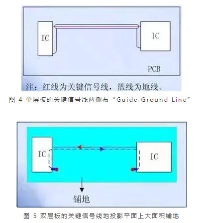
“Guide Ground Line” should be laid on both sides of the key signal line of the single-layer board, as shown in Figure 4. The key signal line of the double-layer board should have a large area of ground on the projection plane, or the same method as the single-layer board, design "Guide Ground Line", as shown in Figure 5. The "guard ground wire" on both sides of the key signal line can reduce the signal loop area on the one hand, and also prevent crosstalk between the signal line and other signal lines.
PCB layout skills
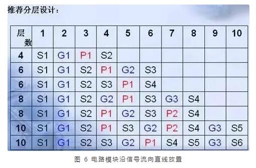
When designing the PCB layout, you should fully observe the design principle of placing in a straight line along the signal flow direction, and try to avoid looping back and forth, as shown in Figure 6. This can avoid direct signal coupling and affect signal quality.
In addition, in order to prevent mutual interference and coupling between circuits and electronic components, the placement of circuits and the layout of components should follow the following principles:
1. If a "clean ground" interface is designed on the board, the filtering and isolation components should be placed on the isolation band between the "clean ground" and the working ground. This can prevent the filtering or isolation devices from coupling to each other through the planar layer, which weakens the effect. In addition, on the "clean ground", apart from filtering and protection devices, no other devices can be placed.
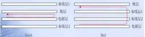
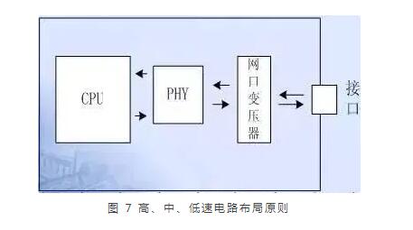
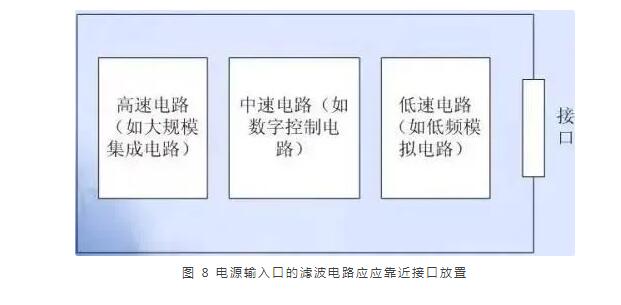
2. When multiple module circuits are placed on the same PCB, digital circuits and analog circuits, high-speed and low-speed circuits should be laid out separately to avoid mutual interference between digital circuits, analog circuits, high-speed circuits, and low-speed circuits. In addition, when high, medium, and low-speed circuits exist on the circuit board at the same time, in order to avoid high-frequency circuit noise from radiating out through the interface, the layout principle in Figure 7 should be .
3. The filter circuit of the power input port of the circuit board should be placed close to the interface to avoid re-coupling of the filtered circuit.
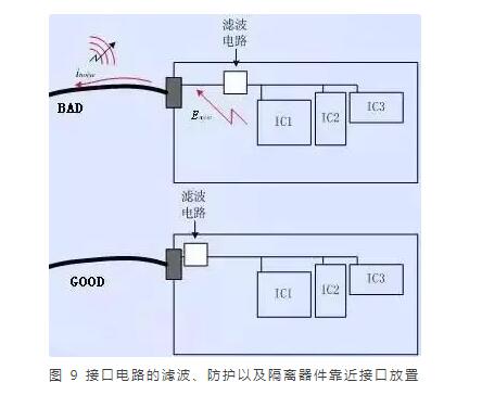
4. The filtering, protection and isolation components of the interface circuit are placed close to the interface, as shown in Figure 9, which can effectively achieve the effects of protection, filtering and isolation. If there is both a filter and a protection circuit at the interface, the principle of first protection and then filtering should be . Because the protection circuit is used for external overvoltage and overcurrent suppression, if the protection circuit is placed after the filter circuit, the filter circuit will be damaged by overvoltage and overcurrent.
In addition, since the input and output lines of the circuit will weaken the filtering, isolation or protection effect when they are coupled with each other, ensure that the input and output lines of the filter circuit (filter), isolation and protection circuit do not couple with each other during layout.
5. Sensitive circuits or components (such as reset circuits, etc.) should be at least 1000 mils away from each edge of the board, especially the edge of the board interface.
6. Energy storage and high-frequency filter capacitors should be placed near the unit circuits or devices with large current changes (such as the input and output terminals of the power supply module, fans and relays) to reduce the loop area of the large current loops.
7. The filter components should be placed side by side to prevent the filtered circuit from being interfered again.
8. Keep strong radiation devices such as crystals, crystal oscillators, relays, switching power supplies, etc. away from the board interface connector at least 1000 mils. In this way, the interference can be directly radiated to the outside or the current can be coupled to the outgoing cable to radiate to the outside.
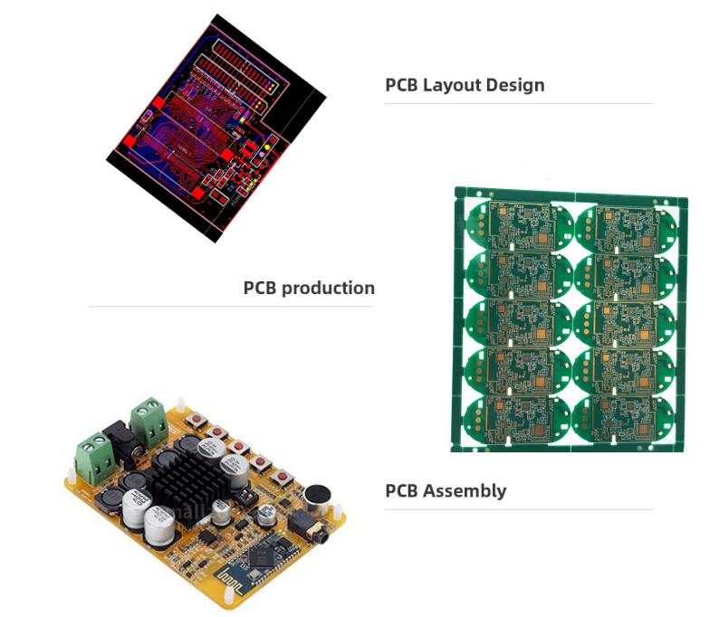
REALTER: Printed Circuit Board, PCB Design, PCB Assembly


 Englishen


