Printed circuit board is made up of layers of copper foil circuits, and the connections between different circuit layers rely on these "vias". This is because today's circuit board manufacturing uses drilled holes to connect different circuits. Between the circuit layers, it is similar to the connection channel of the multi-layer underground waterway. Friends who have played the "Brother Mary" video game may be aware of the connection of water pipes. The difference is that water pipes are required to allow water to circulate ( It’s not to be drilled for Brother Mary), and the purpose of the circuit board connection is to conduct electricity for electrical characteristics, so it is called a via hole, but if you only use a drill or a laser to drill the hole, it will not conduct electricity. Therefore, a layer of conductive material (usually "copper") must be electroplated on the surface of the drilled hole, so that electrons can move between different copper foil layers, because the surface of the original drilled hole is only the resin that does not conduct electricity of.
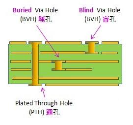
Through hole: Plating Through Hole referred to as PTH
This is the most common type of via hole. You only need to pick up the PCB and face the light, the hole that can see the bright light is the "through hole". This is also the simplest type of hole, because when making it, you only need to use a drill or a laser to directly drill the circuit board, and the cost is relatively cheap. But on the other hand, some circuit layers do not need to connect these through holes. For example, we have a six-story house. The working bear has a lot of money. I bought its third and fourth floors. Then, the working bear himself is on the third floor. A staircase is designed between the fourth floor to communicate with each other, and the working bear does not need to connect to other floors. At this time, if another staircase is designed to pass through each floor from the first to the sixth floor, it will be wasted. With the current circuit board Inch gold should not be allowed. So although through holes are cheap, they sometimes use up more PCB space.
Blind Hole: Blind Via Hole (BVH)
The outermost circuit of the PCB is connected to the adjacent inner layer with a plated hole, but it is not through, because the opposite side cannot be seen, so it is called a "blind hole". In order to increase the space utilization of the PCB circuit layer, a "blind via" process has emerged. This manufacturing method requires special attention to the depth of the drilling (Z axis) to be just right, but this method often causes difficulties in electroplating in the hole, so almost no manufacturer has adopted it.
It is also possible to drill holes for the circuit layers that need to be connected in the individual circuit layers in advance, and then glue them together. The 2+4 board is on, but this requires a more precise positioning and alignment device.
Take the above example of buying a building. A six-story house has only the stairs connecting the first floor and the second floor, or the stairs connecting the fifth floor to the sixth floor, which are called blind holes.
"Blind holes" are holes that can be seen from one side of the board's appearance, but not the other side of the board.
Buried via: Buried Via Hole (BVH)
Any circuit layer inside the PCB is connected but not connected to the outer layer. This process cannot be achieved by drilling after bonding. It must be drilled for individual circuit layers. After the inner layer is partially bonded, it must be electroplated before it can be fully bonded. Compared with the original "through hole" And "blind holes" are more labor-intensive, so the price is the most expensive. This process is usually only used for high-density (HDI) circuit boards to increase the usable space of other circuit layers. Take the example of buying a building above. A six-story house only has stairs connecting the third and fourth floors, which are called buried holes.
"Buried hole" means that the hole cannot be seen from the appearance of the board, but the actual hole is buried in the inner layer of the circuit board.


 Englishen


