Vias in the circuit board are called vias, which are divided into through holes, blind holes and buried holes(HDI Circuit Board). They are mainly used to connect wires on different layers of the same network and are generally not used as soldering components;
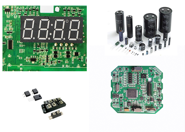
The pads in the circuit board are called pads, which are divided into pin pads and surface mount pads; pin pads have solder holes, which are mainly used for soldering pin components; while surface mount pads have no solder holes and are mainly used for soldering Surface mount components.
Via mainly plays the role of electrical connection, the aperture of via is generally small, usually as long as the board processing technology can do it is enough, and the surface of the via can be coated with solder mask ink or not; while the pad is not only used for electrical The role of connection, but also the role of mechanical fixation, the aperture of the pad (of course refers to the pin pad) must be large enough to pass through the pin of the component, otherwise it will cause production problems; in addition, the surface of the pad must not have Solder mask ink, because it will affect the soldering, and generally the surface of the pad is coated with flux when making the board; and the diameter of the pad's aperture (when referring to the pin pad) must meet a certain Otherwise, it will not only affect the welding, but also cause the installation to be unstable.


 Englishen


