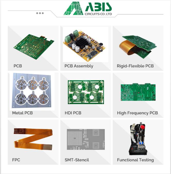
If you are wondering what exactly Printed Circuit Boards (PCBs) are and how they are manufactured, then you are not alone. Many people have a vague understanding of "Circuit Boards", but really aren't experts when it comes to being able to explain what a Printed Circuit Board is. PCBs are usually used to support and electronically connect the connected electronic components to the board. Some examples of electronic components for PCB's are capacitors and resistors. These and other various electronic components are connected through conductive pathways, tracks or signal traces that are etched from sheets of copper that are laminated onto non conductive substrate. When the board has these conductive and non conductive pathways, the boards are sometimes then referred to as Printed Wiring Board (PWB). Once the board has the wiring and electronic components connected, the Printed Circuit Board is now called a Printed Circuit Assembly (PCA) or Printed Circuit Board Assembly (PCBA).
Printed Circuit Boards are most of the time inexpensive, but are still extremely reliable. The initial cost is high because the layout effort requires a lot of time and resources, but PCBs are still a more cost affective and faster to manufacture for high volume production. Many of the industry's PCB Design, quality control, and assembly standards are set by the Association Connecting Electronics Industries (IPC) organization.
When manufacturing PCBs, the majority of printed circuits are produced by bonding a copper layer over the substrate, sometimes on both of the sides, which creates a blank PCB. Then, the unwanted copper is removed after the temporary mask has been applied by etching. This only leaves the copper traces that were desired to remain on the PCB. Depending on if the volume of production is for Sample/Prototype quantities or production volume, there is a process of multiple electroplating, which is a complex process that adds traces or a thin copper layer of substrate onto the bare substrate.
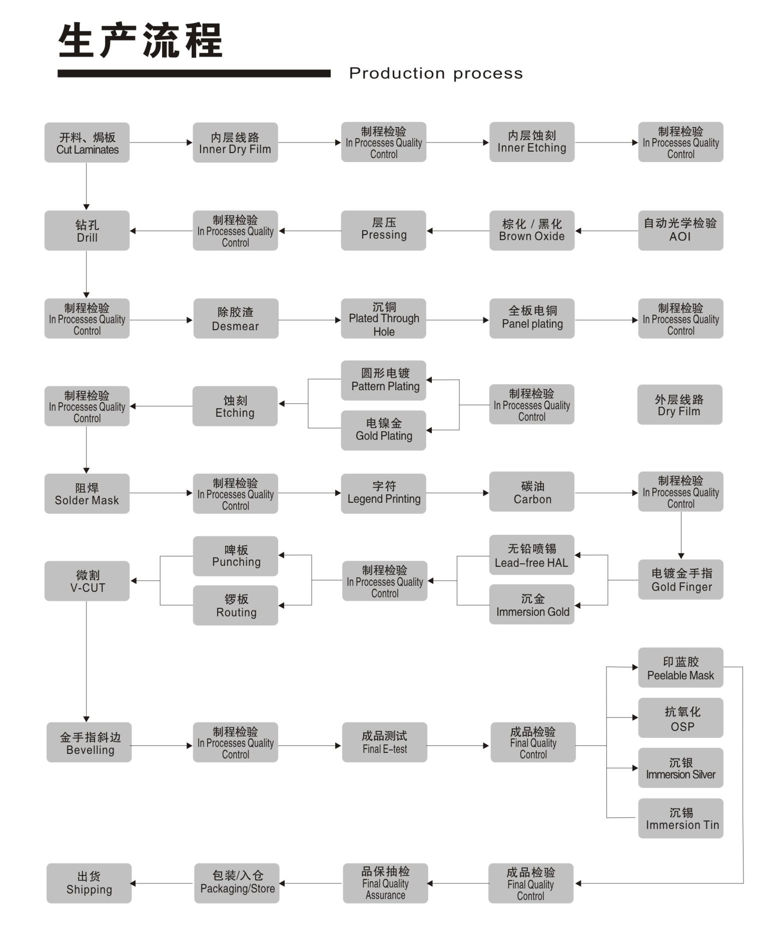
There are various ways to methods for subtractive (or the removal of unwanted copper on the board) during production of the PCBs. The main commercial method of production volume quantities is silk screen printing and photographic methods (Usually used when the line widths are fine). When the production volume is of small quantities, the main methods of used are laser printed resist, print onto transparent film, laser resist ablation, and using a CNC-mill. The most common methods are silk screen printing, photoengraving, and milling. However, there is a common process that also exists that is commonly used for multilayer circuit boards because it facilitates the plating-through of the holes, which is called "Addictive" or "Semi-Addictive".


 Englishen


