Since COB does not have a lead frame of IC package, but is replaced by PCB, the design of PCB pads is very important, and Finish can only use electroplated gold or ENIG, otherwise gold wire or aluminum wire, or even The latest copper wires will have problems that cannot be hit.
PCB Design Requirements for COB
1. The finished surface treatment of the PCB board must be gold electroplating or ENIG, and it is a little thicker than the gold plating layer of the general PCB board, so as to provide the energy required for Die Bonding and form a gold-aluminum or gold-gold total gold.
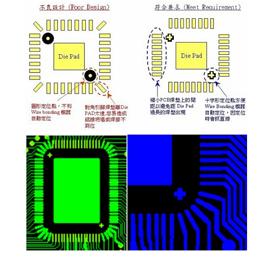
2. In the wiring position of the pad circuit outside the Die Pad of the COB, try to consider that the length of each welding wire has a fixed length, that is to say, the distance of the solder joint from the wafer to the PCB pad should be as consistent as possible. The position of each bonding wire can be controlled to reduce the problem of short circuit when the bonding wires intersect. Therefore, the pad design with diagonal lines does not meet the requirements. It is suggested that the PCB pad spacing can be shortened to eliminate the appearance of diagonal pads. It is also possible to design elliptical pad positions to evenly disperse the relative positions between the bond wires.
3. It is recommended that a COB wafer should have at least two positioning points. It is best not to use the circular positioning points of the traditional SMT, but to use the cross-shaped positioning points, because the Wire Bonding (wire bonding) machine is doing automatic When positioning, the positioning is basically done by grasping the straight line. I think this is because there is no circular positioning point on the traditional lead frame, but only a straight outer frame. Maybe some Wire Bonding machines are not the same. It is recommended to first refer to the performance of the machine to make the design.
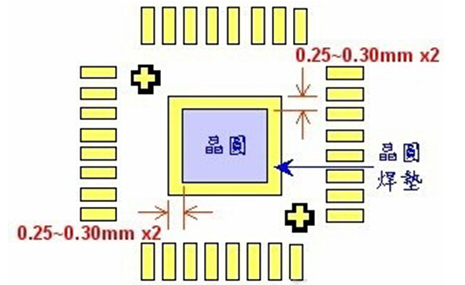
4, the size of the die pad of the PCB should be a little larger than the actual wafer, which can limit the offset when placing the wafer, and also prevent the wafer from rotating too much in the die pad. It is recommended that the wafer pads on each side be 0.25~0.3mm larger than the actual wafer.
5. It is best not to have through holes in the area where the COB needs to be filled with glue. If it cannot be avoided, the PCB factory is required to completely plug these through holes. The purpose is to prevent the through holes from penetrating into the PCB during Epoxy dispensing. on the other side, causing unnecessary problems.
6. It is recommended to print the Silkscreen logo on the area that needs to be dispensed, which can facilitate the dispensing operation and the dispensing shape control.
If you any any question or inquiry, please contact us! Here.
Know more about us! Here.


 Englishen


