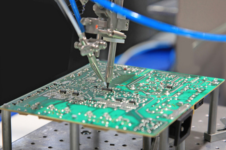
SMT(Printed Circuit Board Assembly, PCBA) is also called surface mount technology. During the manufacturing process, the solder paste is heated and melted in a heating environment, so that the PCB pads are reliably combined with surface mount components through the solder paste alloy. We call this process reflow soldering. Most of the circuit boards are prone to board bending and warping when undergoing Reflow (reflow soldering). In severe cases, it may even cause components such as empty soldering and tombstones.
In the automated assembly line, if the PCB of the circuit board factory is not flat, it will cause inaccurate positioning, components cannot be inserted into the holes and surface mount pads of the board, and even the automatic insertion machine will be damaged. The board with the components is bent after welding, and the component feet are difficult to cut neatly. The board cannot be installed on the chassis or the socket inside the machine, so it is also very annoying for the assembly plant to encounter the board warping. At present, printed boards have entered the era of surface mounting and chip mounting, and assembly plants must have stricter and stricter requirements for board warping.
According to the US IPC-6012 (1996 Edition) "Specification and Performance Specification for Rigid Printed Boards", the maximum allowable warpage and distortion for surface-mounted printed boards is 0.75%, and 1.5% for other boards. Compared with IPC-RB-276 (1992 edition), this has improved the requirements for surface-mounted printed boards. At present, the warpage allowed by various electronic assembly plants, regardless of double-sided or multi-layer, 1.6mm thickness, is usually 0.70~0.75%.
For many SMT and BGA boards, the requirement is 0.5%. Some electronic factories are urging to increase the standard of warpage to 0.3%. The method of testing warpage is in accordance with GB4677.5-84 or IPC-TM-650.2.4.22B. Put the printed board on the verified platform, insert the test pin to the place where the degree of warpage is the greatest, and divide the diameter of the test pin by the length of the curved edge of the printed board to calculate the warpage of the printed board. The curvature is gone.

So in the process of PCB manufacturing, what are the reasons for the bending and warping of the board?
The cause of each plate bending and plate warping may be different, but it should all be attributed to the stress applied to the plate that is greater than the stress that the plate material can withstand. When the plate is subjected to uneven stress or When the ability of each place on the board to resist stress is uneven, the result of board bending and board warping will occur. The following is a summary of the four major causes of plate bending and plate warping.
1. The uneven copper surface area on the circuit board will worsen the bending and warping of the board
Generally, a large area of copper foil is designed on the circuit board for grounding purposes. Sometimes a large area of copper foil is also designed on the Vcc layer. When these large area copper foils cannot be evenly distributed on the same circuit board At this time, it will cause the problem of uneven heat absorption and heat dissipation. Of course, the circuit board will also expand and contract with heat. If the expansion and contraction cannot be performed at the same time, it will cause different stress and deformation. At this time, if the temperature of the board has reached Tg The upper limit of the value, the board will begin to soften, causing permanent deformation.
2. The weight of the circuit board itself will cause the board to dent and deform
Generally, the reflow furnace uses a chain to drive the circuit board forward in the reflow furnace, that is, the two sides of the board are used as fulcrums to support the entire board. If there are heavy parts on the board, or the size of the board is too large, It will show a depression in the middle due to the amount of seed, causing the plate to bend.
3. The depth of the V-Cut and the connecting strip will affect the deformation of the jigsaw
Basically, V-Cut is the culprit that destroys the structure of the board, because V-Cut cuts V-shaped grooves on the original large sheet, so the V-Cut is prone to deformation.
4. The connection points (vias) of each layer on the circuit board will limit the expansion and contraction of the board
Today's circuit boards are mostly multi-layer boards, and there will be rivet-like connection points (via) between layers. The connection points are divided into through holes, blind holes and buried holes. Where there are connection points, the board will be restricted. The effect of expansion and contraction will also indirectly cause plate bending and plate warping.
So how can we better prevent the problem of board warping during the manufacturing process? Here are a few effective methods that I hope can help you.
1. Reduce the effect of temperature on the stress of the board
Since "temperature" is the main source of board stress, as long as the temperature of the reflow oven is lowered or the rate of heating and cooling of the board in the reflow oven is slowed, the occurrence of plate bending and warpage can be greatly reduced. However, other side effects may occur, such as solder short circuit.
2. Using high Tg sheet
Tg is the glass transition temperature, that is, the temperature at which the material changes from the glass state to the rubber state. The lower the Tg value of the material, the faster the board starts to soften after entering the reflow oven, and the time it takes to become soft rubber state It will also become longer, and the deformation of the board will of course be more serious. The use of a higher Tg sheet can increase its ability to withstand stress and deformation, but the price of the relative material is also higher.

3. Increase the thickness of the circuit board
In order to achieve the purpose of lighter and thinner for many electronic products, the thickness of the board has left 1.0mm, 0.8mm, or even 0.6mm. Such a thickness must keep the board from deforming after the reflow furnace, which is really difficult. It is recommended that if there is no requirement for lightness and thinness, the thickness of the board should be 1.6mm, which can greatly reduce the risk of bending and deformation of the board.
4. Reduce the size of the circuit board and reduce the number of puzzles
Since most of the reflow furnaces use chains to drive the circuit board forward, the larger the size of the circuit board will be due to its own weight, dent and deformation in the reflow furnace, so try to put the long side of the circuit board as the edge of the board. On the chain of the reflow furnace, the depression and deformation caused by the weight of the circuit board can be reduced. The reduction in the number of panels is also based on this reason. That is to say, when passing the furnace, try to use the narrow edge to pass the furnace direction as far as possible. The amount of depression deformation.
5. Used furnace tray fixture
If the above methods are difficult to achieve, the last is to use reflow carrier/template to reduce the amount of deformation. The reason why the reflow carrier/template can reduce the bending of the plate is because it is hoped whether it is thermal expansion or cold contraction. The tray can hold the circuit board and wait until the temperature of the circuit board is lower than the Tg value and start to harden again, and it can also maintain the original size.
If the single-layer pallet cannot reduce the deformation of the circuit board, a cover must be added to clamp the circuit board with the upper and lower pallets. This can greatly reduce the problem of circuit board deformation through the reflow furnace. However, this furnace tray is quite expensive, and manual labor is required to place and recycle the trays.
6. Use Router instead of V-Cut to use the sub-board
Since V-Cut will destroy the structural strength of the board between the circuit boards, try not to use the V-Cut sub-board or reduce the depth of the V-Cut.
7. Three points run through in engineering design:
A. The arrangement of interlayer prepregs should be symmetrical, for example, for six-layer boards, the thickness between 1~2 and 5~6 layers and the number of prepregs should be the same, otherwise it is easy to warp after lamination.
B. Multi-layer core board and prepreg should use the same supplier's products.
C. The area of the circuit pattern on side A and side B of the outer layer should be as close as possible. If the A side is a large copper surface, and the B side only has a few lines, this kind of printed board will easily warp after etching. If the area of the lines on the two sides is too different, you can add some independent grids on the thin side for balance.
8. The latitude and longitude of the prepreg:
After the prepreg is laminated, the warp and weft shrinkage rates are different, and the warp and weft directions must be distinguished during blanking and lamination. Otherwise, it is easy to cause the finished board to warp after lamination, and it is difficult to correct it even if the pressure is applied to the baking board. Many reasons for the warpage of the multilayer board are that the prepregs are not distinguished in the warp and weft directions during lamination, and they are stacked randomly.
The method to distinguish the warp and weft directions: the rolling direction of the prepreg in a roll is the warp direction, while the width direction is the weft direction; for the copper foil board, the long side is the weft direction and the short side is the warp direction. If you are not sure, please contact the manufacturer Or supplier query.
9. Baking board before cutting:
The purpose of baking the board before cutting the copper clad laminate (150 degrees Celsius, time 8±2 hours) is to remove the moisture in the board, and at the same time make the resin in the board completely solidify, and further eliminate the remaining stress in the board, which is useful for preventing the board from warping. Helping. At present, many double-sided and multi-layer boards still adhere to the step of baking before or after the blanking. However, there are exceptions for some plate factories. The current PCB drying time regulations of various PCB factories are also inconsistent, ranging from 4 to 10 hours. It is recommended to decide according to the grade of the printed board produced and the customer's requirements for warpage. Bake after cutting into a jigsaw or blanking after the whole block is baked. Both methods are feasible. It is recommended to bake the board after cutting. The inner layer board should also be baked...
10. In addition to stress after lamination:
After the multi-layer board is hot-pressed and cold-pressed, it is taken out, cut or milled off the burrs, and then placed flat in an oven at 150 degrees Celsius for 4 hours, so that the stress in the board is gradually released and the resin is completely cured. This step cannot be omitted.
11. The thin plate needs to be straightened during electroplating:
When the 0.4~0.6mm ultra-thin multilayer board is used for surface electroplating and pattern electroplating, special clamping rollers should be made. After the thin plate is clamped on the fly bus on the automatic electroplating line, a round stick is used to clamp the entire fly bus. The rollers are strung together to straighten all the plates on the rollers so that the plates after plating will not be deformed. Without this measure, after electroplating a copper layer of 20 to 30 microns, the sheet will bend and it is difficult to remedy it.
12. Cooling of the board after hot air leveling:
When the printed board is leveled by hot air, it is impacted by the high temperature of the solder bath (about 250 degrees Celsius). After being taken out, it should be placed on a flat marble or steel plate for natural cooling, and then sent to a post-processing machine for cleaning. This is good for preventing warpage of the board. In some factories, in order to enhance the brightness of the lead-tin surface, the boards are put into cold water immediately after the hot air is leveled, and then taken out after a few seconds for post-processing. This kind of hot and cold impact may cause warping on certain types of boards. Twisted, layered or blistered. In addition, an air flotation bed can be installed on the equipment for cooling.
13. Treatment of warped board:
In a well-managed factory, the printed board will be 100% flatness checked during the final inspection. All unqualified boards will be picked out, put in the oven, baked at 150 degrees Celsius under heavy pressure for 3-6 hours, and cooled naturally under heavy pressure. Then relieve the pressure to take out the board, and check the flatness, so that part of the board can be saved, and some boards need to be bake and pressed two or three times before they can be leveled. If the above-mentioned anti-warping process measures are not implemented, some of the boards will be useless and can only be scrapped.


 Englishen


