Ceramic circuit boards are actually made of electronic ceramic materials and can be made into various shapes. Among them, the ceramic circuit board has the most outstanding characteristics of high temperature resistance and high electrical insulation. It has the advantages of low dielectric constant, low dielectric loss, high thermal conductivity, good chemical stability, and similar thermal expansion coefficients of components. Ceramic printed circuit boards are produced using laser rapid activation metallization technology LAM technology. Used in the LED field, high-power semiconductor modules, semiconductor coolers, electronic heaters, power control circuits, power hybrid circuits, smart power components, high-frequency switching power supplies, solid state relays, automotive electronics, communications, aerospace and military electronic components.
Different from traditional FR-4 (glass fiber), ceramic materials have good high-frequency performance and electrical properties, as well as high thermal conductivity, chemical stability and thermal stability. Ideal packaging materials for the production of large-scale integrated circuits and power electronic modules.
Main advantages:
1. Higher thermal conductivity
2. More matching thermal expansion coefficient
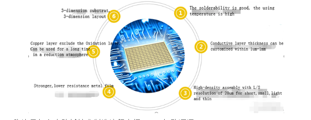
3. A harder, lower resistance metal film alumina ceramic circuit board
4. The solderability of the base material is good, and the use temperature is high.
5. Good insulation
6. Low frequency loss
7. Assemble with high density
8. It does not contain organic ingredients, is resistant to cosmic rays, has high reliability in aerospace and aerospace, and has a long service life
9. The copper layer does not contain an oxide layer and can be used for a long time in a reducing atmosphere.
Technical advantages
Introduction to the manufacturing process of ceramic printed circuit board technology-hole punching
With the development of high-power electronic products in the direction of miniaturization and high-speed, traditional FR-4, aluminum substrate and other substrate materials are no longer suitable for the development of high-power and high-power.
With the advancement of science and technology, the intelligent application of PCB industry. The traditional LTCC and DBC technologies are gradually replaced by DPC and LAM technologies. The laser technology represented by LAM technology is more in line with the development of high-density interconnection and fineness of printed circuit boards. Laser drilling is the front-end and mainstream drilling technology in the PCB industry. The technology is efficient, fast, accurate, and has high application value.
The RayMingceramic circuit board is made with laser rapid activation metallization technology. The bonding strength between the metal layer and the ceramic is high, the electrical properties are good, and the welding can be repeated. The thickness of the metal layer can be adjusted in the range of 1μm-1mm, which can achieve L/S resolution. 20μm, can be directly connected to provide customized solutions for customers
Lateral excitation of atmospheric CO2 laser is developed by a Canadian company. Compared with traditional lasers, the output power is as high as one hundred to one thousand times, and it is easy to manufacture.
In the electromagnetic spectrum, the radio frequency is in the frequency range of 105-109 Hz. With the development of military and aerospace technology, the secondary frequency is emitted. Low and medium power RF CO2 lasers have excellent modulation performance, stable power and high operational reliability. Features such as long life. UV solid YAG is widely used in plastics and metals in the microelectronics industry. Although the CO2 laser drilling process is more complicated, the production effect of the micro-aperture is better than that of UV solid YAG, but the CO2 laser has the advantages of high efficiency and high-speed punching. The market share of PCB laser micro-hole processing can be domestic laser micro-hole manufacturing is still developing At this stage, not many companies can put into production.
Domestic laser microvia manufacturing is still in the development stage. Short pulse and high peak power lasers are used to drill holes in PCB substrates to achieve high-density energy, material removal and micro-hole formation. Ablation is divided into photothermal ablation and photochemical ablation. Photothermal ablation refers to the completion of the hole formation process through the rapid absorption of high-energy laser light by the substrate material. Photochemical ablation refers to the combination of high photon energy in the ultraviolet region exceeding 2 eV electron volts and laser wavelength exceeding 400 nm. The manufacturing process can effectively destroy the long molecular chains of organic materials to form smaller particles, and the particles can quickly form micropores under the action of external force.
Today, China's laser drilling technology has certain experience and technological progress. Compared with traditional stamping technology, laser drilling technology has high precision, high speed, high efficiency, large-scale batch punching, suitable for most soft and hard materials, without loss of tools, and waste generation. The advantages of less materials, environmental protection and no pollution.
The ceramic circuit board is through the laser drilling process, the bonding force between the ceramic and the metal is high, does not fall off, foaming, etc., and the effect of growth together, high surface flatness, roughness ratio of 0.1 micron to 0.3 micron, laser strike hole diameter From 0.15 mm to 0.5 mm, or even 0.06 mm.
Ceramic circuit board manufacturing-etching
The copper foil remaining on the outer layer of the circuit board, that is, the circuit pattern, is pre-plated with a layer of lead-tin resist, and then the unprotected non-conductor part of the copper is chemically etched to form a circuit.
According to different process methods, etching is divided into inner layer etching and outer layer etching. The inner layer etching is acid etching, wet film or dry film m is used as a resist; the outer layer etching is alkaline etching, and tin-lead is used as a resist. Agent.
The basic principle of etching reaction
1. Alkalization of acid copper chloride

1, Acidic copper chloride alkalization
Exposure: The part of the dry film that has not been irradiated by ultraviolet rays is dissolved by weak alkaline sodium carbonate, and the irradiated part remains.
Etching: According to a certain proportion of the solution, the copper surface exposed by dissolving the dry film or the wet film is dissolved and etched by the acid copper chloride etching solution.
Fading film: The protective film on the production line dissolves at a certain proportion of specific temperature and speed.
Acidic copper chloride catalyst has the characteristics of easy control of etching speed, high copper etching efficiency, good quality, and easy recovery of etching solution
2. Alkaline etching
Alkaline etching
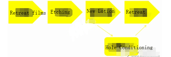
Fading film: Use meringue liquid to remove the film from the film surface, exposing the unprocessed copper surface.
Etching: The unneeded bottom layer is etched away with an etchant to remove the copper, leaving thick lines. Among them, auxiliary equipment will be used. The accelerator is used to promote the oxidation reaction and prevent the precipitation of cuprous ions; the insect repellent is used to reduce the side erosion; the inhibitor is used to inhibit the dispersion of ammonia, the precipitation of copper, and accelerate the oxidation of copper.
New emulsion: Use monohydrate ammonia water without copper ions to remove the residue on the plate with ammonium chloride solution.
Full hole: This procedure is only suitable for immersion gold process. Mainly remove the excessive palladium ions in the non-plated through holes to prevent the gold ions from sinking in the gold precipitation process.
Tin peeling: The tin-lead layer is removed using a nitric acid solution.
Four effects of etching
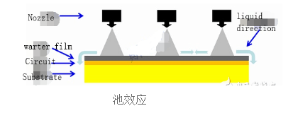
1. Pool effect
During the etching manufacturing process, the liquid will form a water film on the board due to gravity, thereby preventing the new liquid from contacting the copper surface.
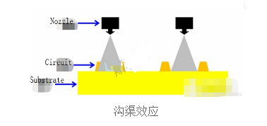
2. Groove effect
The adhesion of the chemical solution causes the chemical solution to adhere to the gap between the pipeline and the pipeline, which will result in a different etching amount in the dense area, and the open area.
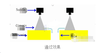
3. Pass effect
The liquid medicine flows downward through the hole, which increases the renewal speed of the liquid medicine around the plate hole during the etching process, and the etching amount increases.
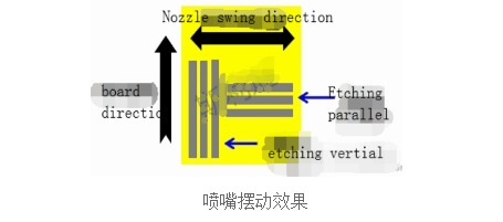
4. Nozzle swing effect
The line parallel to the swing direction of the nozzle, because the new liquid medicine can easily dissipate the liquid medicine between the lines, the liquid medicine is quickly updated, and the amount of etching is large;
The line perpendicular to the swing direction of the nozzle, because the new chemical liquid is not easy to dissipate the liquid medicine between the lines, the liquid medicine is refreshed at a slower speed, and the etching amount is small.
Common problems in etching production and improvement methods
1. The movie is endless
Because the concentration of the syrup is very low; the linear velocity is too fast; the nozzle clogging and other problems will cause the film to be endless. Therefore, it is necessary to check the concentration of the syrup and adjust the concentration of the syrup to an appropriate range; adjust the speed and parameters in time; then clean the nozzle.
2. The surface of the board is oxidized
Because the syrup concentration is too high and the temperature is too high, it will cause the surface of the board to oxidize. Therefore, it is necessary to adjust the concentration and temperature of the syrup in time.
3. Thetecopper is not completed
Because the etching speed is too fast; the composition of the syrup is biased; the copper surface is contaminated; the nozzle is blocked; the temperature is low and the copper is not completed. Therefore, it is necessary to adjust the etching transmission speed; recheck the composition of the syrup; be careful of copper contamination; clean the nozzle to prevent clogging; adjust the temperature.
4. The etching copper is too high
Because the machine runs too slowly, the temperature is too high, etc., it may cause excessive copper corrosion. Therefore, measures such as adjusting the machine speed and adjusting the temperature should be taken.


 Englishen


